- 您现在的位置:买卖IC网 > Sheet目录345 > MT42L256M32D4KP-3 IT:A (Micron Technology Inc)IC LPDDR2 SDRAM 8GBIT 168FBGA
�� �
�
�2Gb:� x16,� x32� Mobile� LPDDR2� SDRAM� S4�
�Data� Setup,� Hold,� and� Slew� Rate� Derating�
�Data� Setup,� Hold,� and� Slew� Rate� Derating�
�For� all� input� signals� (DQ,� DM)� calculate� the� total� required� setup� time� (� t� DS)� and� hold�
�time� (� t� DH)� by� adding� the� data� sheet� t� DS(base)� and� t� DH(base)� values� (see� Table� 92�
�(page� 156))� to� the� Δ� t� DS� and� Δ� t� DH� derating� values,� respectively� (see� Table� 94� and� Ta-�
�ble� 95� (page� 157)).� Example:� t� DS� =� t� DS(base)� +� Δ� t� DS.�
�The� typical� t� DS� slew� rate� for� a� rising� signal� is� defined� as� the� slew� rate� between� the� last�
�crossing� of� V� REF(DC)� and� the� first� crossing� of� V� IH(AC)min� .� The� typical� t� DS� slew� rate� for� a�
�falling� signal� is� defined� as� the� slew� rate� between� the� last� crossing� of� V� REF(DC)� and� the�
�first� crossing� of� V� IL(AC)max� (see� Figure� 101� (page� 159)).�
�If� the� actual� signal� is� consistently� earlier� than� the� typical� slew� rate� line� in� Figure� 97�
�(page� 152)� the� area� shaded� gray� between� the� V� REF(DC)� region� and� the� AC� region,� use� the�
�typical� slew� rate� for� the� derating� value.� If� the� actual� signal� is� later� than� the� typical� slew�
�rate� line� anywhere� between� the� shaded� V� REF(DC)� region� and� the� AC� region,� the� slew� rate�
�of� a� tangent� line� to� the� actual� signal� from� the� AC� level� to� the� DC� level� is� used� for� the�
�derating� value� (see� Figure� 99� (page� 154)).�
�The� typical� t� DH� slew� rate� for� a� rising� signal� is� defined� as� the� slew� rate� between� the� last�
�crossing� of� V� IL(DC)max� and� the� first� crossing� of� V� REF(DC)� .� The� typical� t� DH� slew� rate� for� a�
�falling� signal� is� defined� as� the� slew� rate� between� the� last� crossing� of� V� IH(DC)min� and� the�
�first� crossing� of� V� REF(DC)� (see� Figure� 102� (page� 160)).�
�If� the� actual� signal� is� consistently� later� than� the� typical� slew� rate� line� between� the�
�shaded� DC-level-to-V� REF(DC)� region,� use� the� typical� slew� rate� for� the� derating� value.� If�
�the� actual� signal� is� earlier� than� the� typical� slew� rate� line� anywhere� between� shaded� DC-�
�to-V� REF(DC)� region,� the� slew� rate� of� a� tangent� line� to� the� actual� signal� from� the� DC� level�
�to� the� V� REF(DC)� level� is� used� for� the� derating� value� (see� Figure� 104� (page� 162)).�
�For� a� valid� transition,� the� input� signal� must� remain� above� or� below� V� IH� /V� IL(AC)� for� the�
�specified� time,� t� VAC� (see� Table� 96� (page� 158)).�
�The� total� setup� time� for� slow� slew� rates� could� be� negative� (that� is,� a� valid� input� signal�
�may� not� have� reached� V� IH� /V� IL(AC)� at� the� time� of� the� rising� clock� transition).� A� valid� input�
�signal� is� still� required� to� complete� the� transition� and� reach� V� IH� /V� IL(AC)� .�
�For� slew� rates� between� the� values� listed� in� Table� 92� and� Table� 93,� the� derating� values�
�can� be� obtained� using� linear� interpolation.� Slew� rate� values� are� not� typically� subject� to�
�production� testing.� They� are� verified� by� design� and� characterization.�
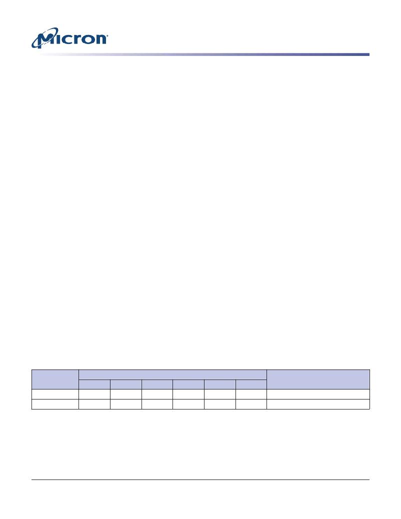
�Table� 92:� Data� Setup� and� Hold� Base� Values� (>400� MHz,� 1� V/ns� Slew� Rate)�
�Data� Rate�
�Parameter�
�1066�
�933�
�800�
�667�
�533�
�466�
�Reference�
�t� DS�
�t� DH�
�(base)�
�(base)�
�-10�
�80�
�15�
�105�
�50�
�140�
�130�
�220�
�210�
�300�
�230�
�320�
�V� IH� /V� IL(AC)� =� V� REF(DC)� ±220mV�
�V� IH� /V� IL(DC)� =� V� REF(DC)� ±130mV�
�Note:�
�1.� AC/DC� referenced� for� 1� V/ns� DQ,� DM� slew� rate,� and� 2� V/ns� differential� DQS/DQS#� slew�
�rate.�
�PDF:� 09005aef83f3f2eb�
�2gb_mobile_lpddr2_s4_g69a.pdf� –� Rev.� N� 3/12� EN�
�156�
�Micron� Technology,� Inc.� reserves� the� right� to� change� products� or� specifications� without� notice.�
�2010� Micron� Technology,� Inc.� All� rights� reserved.�
�发布紧急采购,3分钟左右您将得到回复。
相关PDF资料
MT45W1MW16BDGB-708 AT
IC PSRAM 16MBIT 104MHZ 54VFBGA
MT48H32M16LFB4-75B IT:C
IC SDRAM 512MB 54VFBGA
MT48H8M16LFB4-75 IT:K TR
IC SDRAM 128MBIT 133MHZ 54VFBGA
MTC100-JA2-P34
CONTACT INSERT PIN
MX841BE
IC CONVERTER WHITE LED 8-SOIC
MXHV9910BTR
IC LED DRIVER HIGH BRIGHT 8-SOIC
MXN12FB12F
MOTOR BRUSHED DC 12V 2922RPM
MXN13FB08B1
MOTOR BRUSHED DC 8V 4714RPM
相关代理商/技术参数
MT42L256M32D4KP-MS
制造商:Micron Technology Inc 功能描述:256MX32 LPDDR2 PLASTIC IND TEMP GREEN WFBGA 1.2V - Bulk